Nagare Labs is positioning its new memory architecture to resolve the widening performance gap between AI logic and data access. The Atlanta-based startup, a Georgia Tech spinout, has emerged from stealth with $5M in funding led by Playground Global. This capital aims to advance a technology designed to address the "memory wall," where memory bandwidth growth of 20% annually fails to keep pace with the 70% annual surge in peak compute performance. For enterprise AI, this disparity creates significant bottlenecks in generative AI inference workloads.
Nagare Labs $5M Funding and Georgia Tech Origins
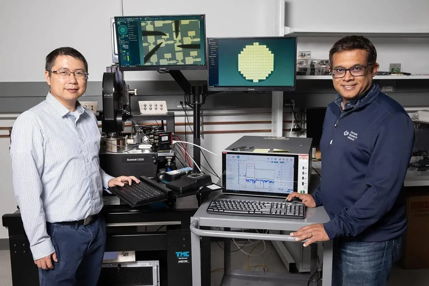
The $5M investment led by Playground Global supports the commercialization of a new memory tier intended to bridge the architectural divide between logic and memory. Nagare Labs was co-founded by Dr. Suman Datta and Dr. Shimeng Yu, researchers from Georgia Tech with significant semiconductor backgrounds. Dr. Datta is a co-inventor of Intel’s High-k/Metal Gate and Tri-gate logic transistor architectures, while Dr. Yu created NeuroSim, an open-source simulator used globally for emerging memory design. The company is targeting the inefficiencies inherent in current frontier systems, where chipmakers and hyperscalers face costly tradeoffs between on-die SRAM and off-die DRAM or High Bandwidth Memory (HBM). While SRAM offers high bandwidth, its scaling has flatlined due to expensive logic die area consumption. Conversely, HBM and DRAM provide capacity but introduce latency, thermal strain, and energy waste during data movement.
Z2RAM Architecture and Manufacturing Compatibility
To address these constraints, Nagare Labs has developed Z2RAM, a transistor-based, capacitor-less architecture. The company claims Z2RAM unifies SRAM-like speed with DRAM-level bit density into a single tier, making it suitable for 3D heterogeneous integration directly on top of logic dies. This approach aims to reduce the energy and time wasted when data shuttles across package and interposer interconnects. Crucially, Nagare is positioning Z2RAM for rapid commercialization by utilizing standard back-end-of-the-line integration processes. By using fab-compatible materials and tools, the architecture avoids the exotic materials that have stalled previous industry attempts. Furthermore, the design is 3D bit cost scalable, allowing multiple layers to be processed via a single lithography exposure without requiring expensive Extreme Ultraviolet (EUV) lithography.
Key Takeaways
- Nagare Labs raised $5M in a funding round led by Playground Global to develop new AI memory technology.
- The company's Z2RAM architecture utilizes a capacitor-less design to combine SRAM-like speed with DRAM-level density.
- Z2RAM is engineered to use standard back-end-of-the-line integration and fab-compatible materials to facilitate manufacturing.
TechInsyte's Take
In our view, Nagare Labs is attempting to solve the most expensive problem in the AI data center: the energy and latency tax of data movement. By focusing on a capacitor-less, 3D-integratable architecture, they are not just proposing a new material, but a new way to stack memory directly onto logic. This is a strategic move to bypass the "memory wall" that currently forces hyperscalers into inefficient, high-cost hardware configurations. If Nagare can successfully leverage existing fab infrastructure without requiring exotic materials or EUV, they may provide a more viable path to scaling generative AI inference than current HBM-centric models.
Questions & Answers
How does Nagare Labs intend to bypass the traditional limitations of HBM and SRAM?
Nagare Labs is developing Z2RAM, a capacitor-less architecture that aims to provide the high speed of SRAM alongside the high bit density of DRAM. This allows for 3D heterogeneous integration on top of logic dies, reducing the latency and energy waste associated with moving data across interconnects.
What makes the Z2RAM architecture commercially viable compared to previous memory innovations?
Unlike previous attempts that relied on exotic materials, Z2RAM utilizes standard back-end-of-the-line integration processes and fab-compatible materials. Additionally, it is designed to be 3D bit cost scalable using a single lithography exposure, avoiding the need for expensive EUV.
What specific market gap is Nagare Labs addressing within the AI hardware sector?
The company is addressing the "memory wall," where compute performance grows at 70% annually while memory bandwidth only grows at 20%. This disparity throttles generative AI inference and forces enterprises to make costly tradeoffs between bandwidth, capacity, and energy efficiency.
Source: Nagare Labs