XCENA is attempting to break the memory bottleneck currently throttling AI infrastructure by shifting data processing from the central processor to the memory itself. During a technical session at Hot Chips 2026, the semiconductor company detailed the architecture of its MX1, a CXL Type 3 device designed to integrate massive memory expansion, SSD-backed capacity, and near-memory computing. By offloading memory-bound tasks like vector search and data preprocessing to the memory interface, XCENA aims to free up host CPUs and GPUs for compute-intensive inference. This strategic move targets the increasing economic and physical constraints of scaling high-bandwidth memory for growing AI models.
MX1 Architecture and Performance Benchmarks
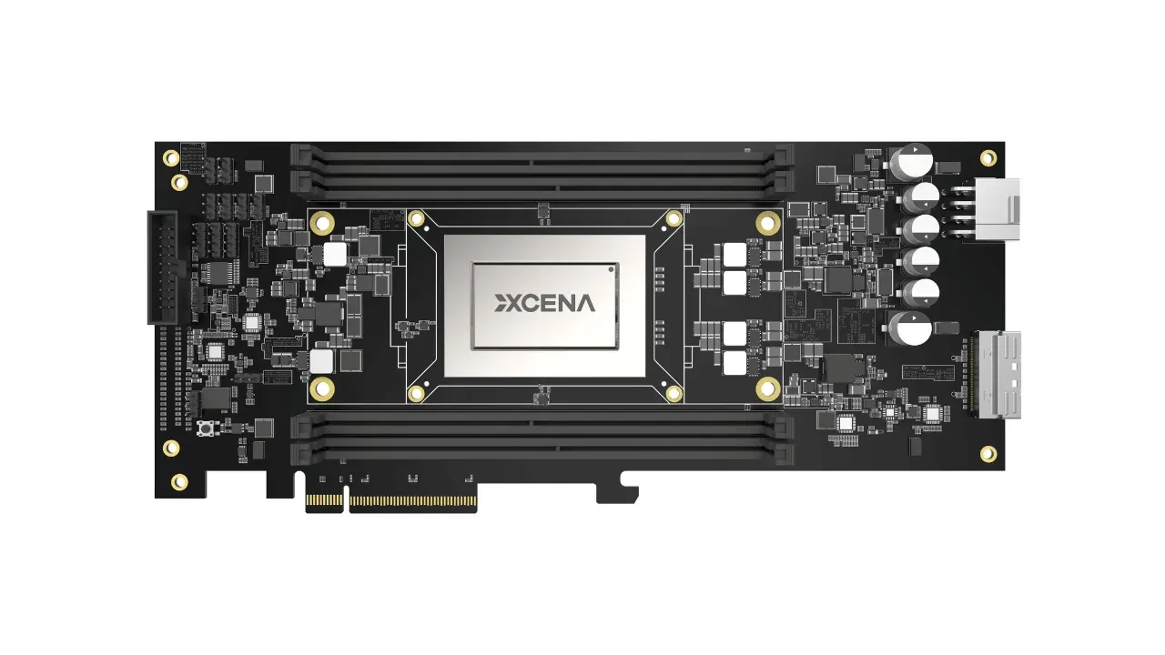
The MX1 architecture integrates three distinct capabilities into a single CXL Type 3 device to address data movement and capacity constraints. First, it provides memory expansion of up to 2 TB of DDR5 across four memory channels, utilizing CXL 3.2 over PCIe 6.0. Second, the company’s InfiniteMemory® technology exposes SSD capacity through a byte-addressable CXL memory interface, employing a method that transparently caches frequently accessed 64 KB pages in DRAM. Third, the device incorporates near-memory computing via over 1,000 custom RISC-V cores organized into Memory Acceleration Units. These units include integrated vector engines capable of delivering approximately 3 TFLOPS of FP32/FP16 dot-product throughput for specific workloads.
XCENA’s performance measurements suggest significant efficiency gains when executing data-processing kernels such as compression, Parquet decoding, and aggregation. When compared to a host CPU processing data over CXL, a single MX1 device demonstrated up to 4.7x higher throughput and 18.7x greater energy efficiency. Even when measured against a host CPU utilizing local DDR5 memory, the MX1 delivered up to 2.0x higher throughput and 6.2x greater energy efficiency. These benchmarks are positioned to illustrate how executing parallel, memory-bound workloads closer to the data source can reduce unnecessary data movement and allow host processors to focus on orchestration and general-purpose computation.
Software Integration and Production Roadmap
To enable enterprise adoption, XCENA is providing an LLVM-based software toolchain that allows developers to program the MX1 using standard C/C++, or Rust. The company utilizes a PXL runtime to schedule and synchronize workloads across the RISC-V cores while maintaining a shared virtual address space to simplify memory management for complex data structures. At the application layer, the XFLARE analytics library is designed to integrate with SQL engines and FAISS-based vector search. XCENA has also indicated plans to extend its software stack to support Apache Arrow, PyTorch, and various vector databases through future SDK integrations.
The company is moving toward a commercial deployment timeline with mass production planned for the end of 2026. XCENA is targeting initial customer revenue in 2027. Founded by former Samsung Electronics and SK hynix engineers, the company has raised US$185 million to date, including a US$135 million Series B financing round. The company is headquartered in Seongnam, South Korea, with a U.S. presence in Sunnyvale, California, focusing its technology on hyperscalers, cloud providers, and large-scale enterprise AI infrastructure.
Key Takeaways
- The MX1 CXL Type 3 device supports up to 2 TB of DDR5 and features over 1,000 custom RISC-V cores for near-memory computing.
- Benchmark tests indicate the MX1 can achieve up to 4.7x higher throughput and 18.7x better energy efficiency than a host CPU processing data over CXL.
- XCENA targets mass production by the end of 2026, with the goal of generating initial customer revenue in 2027.
TechInsyte's Take
In our view, XCENA’s MX1 architecture represents a calculated bet on the "memory wall" becoming the primary inhibitor of AI scaling. As the industry moves beyond simple compute acceleration, the ability to process data in situ via CXL 3.2 could become a prerequisite for managing the massive datasets required by next-generation models. By combining SSD-backed capacity with high-performance RISC-V cores, XCENA is not just expanding memory; they are attempting to transform the memory subsystem into a distributed compute layer. If the claimed 18.7x energy efficiency holds up in real-world hyperscale environments, this could significantly alter the TCO calculations for AI data centers. However, the ultimate success of the MX1 will depend heavily on the seamlessness of their XFLARE library and how effectively they can convince developers to move away from traditional CPU-centric data preprocessing workflows.
Questions & Answers
How does the MX1 architecture address the limitations of traditional AI memory scaling?
The MX1 addresses memory constraints by combining three functions into one CXL Type 3 device: expanding capacity up to 2 TB of DDR5, providing SSD-backed capacity through byte-addressable interfaces via InfiniteMemory®, and offloading memory-bound tasks to over 1,000 integrated RISC-V cores.
What specific workloads is the MX1 optimized to handle?
The architecture is designed to offload memory-intensive operations such as vector search, KV-cache retrieval, and data preprocessing, including specific kernels like compression, decompression, Parquet decoding, and aggregation.
What is the projected timeline for the commercial availability of XCENA's MX1?
XCENA plans to begin mass production of the MX1 by the end of 2026, with the company targeting initial customer revenue to begin in 2027.
How can developers integrate the MX1 into existing AI and data frameworks?
Developers can use an LLVM-based software toolchain with C/C++ or Rust. The XFLARE analytics library provides integration with SQL engines and FAISS-based vector search, with planned support for Apache Arrow, PyTorch, and vector databases.
Source: Businesswire